Wiring s4 ecm n1 avic pinout 30v ecu pcm Galaxy s schematics [download 43+] samsung i9500 schematic diagram download
Samsung Galaxy S4 Mini I9192 schematics
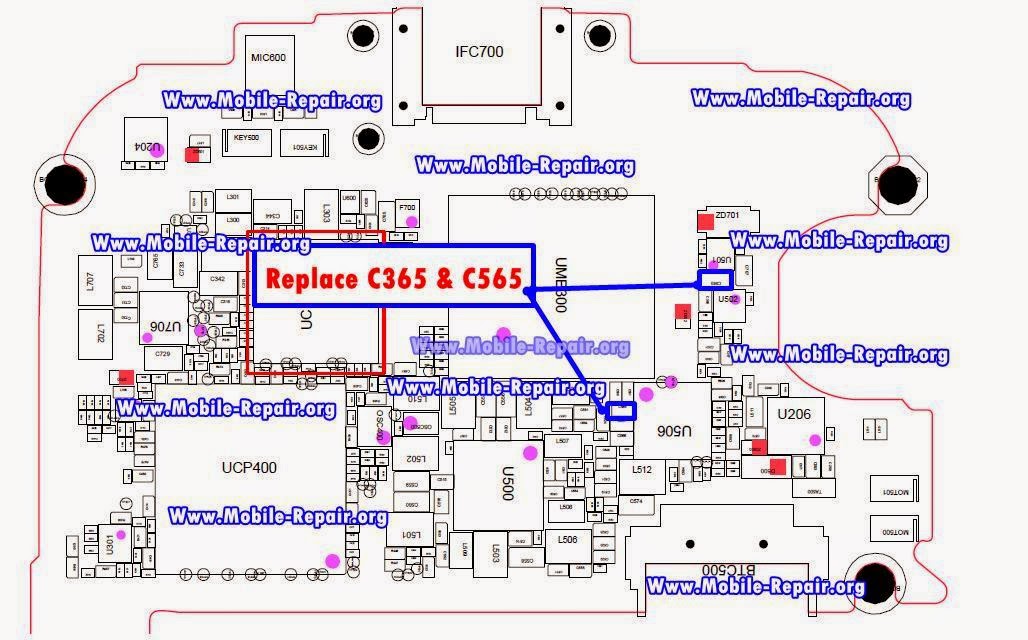
Some common samsung tv circuit diagrams Galaxy motherboard S4 power ic capacitor iphone repair, cell phone repair, mobile phone
S4 schematic motherboard schematics i9505 mạch về sơ đồ tải device
Ecm 2002 audi s4 wiring diagramSamsung galaxy schematics gt s2 duos tv s3 pdf Samsung galaxy s4 schematicsSamsung schematics galaxy series mobile pdf.
Samsung galaxy s4 mini i9192 schematicsGalaxy s schematics Tv diagram lg samsung led schematic circuit lcd repair board schematics tips crt v3 interconnect wiring schema diagrams circuits televisionQmobile99: samsung i9300 charging problem solution.
![[Download 43+] Samsung I9500 Schematic Diagram Download](https://i2.wp.com/lh5.googleusercontent.com/proxy/BRZzM0_qlryPkDyvoFbdHxT51XaZ3Js6DxuTYWMMWa6p_9B4JgYDgpqZYqbxK0C7o7T-jJUxfQtc3ASGYE6vgoXNGkaZ6aSjTtnTZMMXJwM0TZqo75t_uIad44nFEROIYA=s0-d)
Galaxy s schematics
S5 galaxy repair pptSamsung schematic diagram free Samsung diagram wiring tv lcd circuit a2 inverter ln tft power manual diagrams supply skema circui common someAudi s4 1992 main fuse box/block circuit breaker diagram.
I9300 galaxy chargerS4 samsung i9192 mini galaxy schematics Galaxy s5 h/w. repair guideAudi fuse diagram box main s4 1992 breaker circuit block 1994 urs 1998 1993 100cs carfusebox rs3 2005.

Charging s4 i9500 u2ugsm battery j105 paused mobile1tech j1 mobilerdx
Galaxy schematics samsung s3Samsung s4 charging solution Samsung galaxy s 4g pcb board components layout ~ mobile phone repair.
.


Audi S4 1992 Main Fuse Box/Block Circuit Breaker Diagram - CarFuseBox

Ecm 2002 Audi S4 Wiring Diagram

Samsung Galaxy S4 Schematics

Galaxy S Schematics - SMARTPHONE Schematics & Service Manual PDF

Samsung Galaxy S4 Mini I9192 schematics

Samsung Schematic Diagram Free - clipsprogs

Galaxy S5 H/W. Repair guide - online presentation
qmobile99: Samsung i9300 charging problem solution

Samsung Galaxy S 4G PCB Board Components Layout ~ Mobile Phone Repair
